Kulicke & Soffa (K&S) serves the automotive, consumer, communications, computing and industrial markets as a top provider of semiconductor and electronic assembly solutions. The company was established in 1951 and in 1971 became one of the first technology companies listed on the NASDAQ.
NDC International is the North American distributor for K&S brand dicing blades and capillaries. K&S has a complete line of dicing blade solutions for all of your wafer dicing and package singulation needs including the latest technology in both hub and hubless configurations. They aim to provide the best cut quality and blade life for your sawing applications. K&S is committed to improving your profitability by increasing yields and productivity.
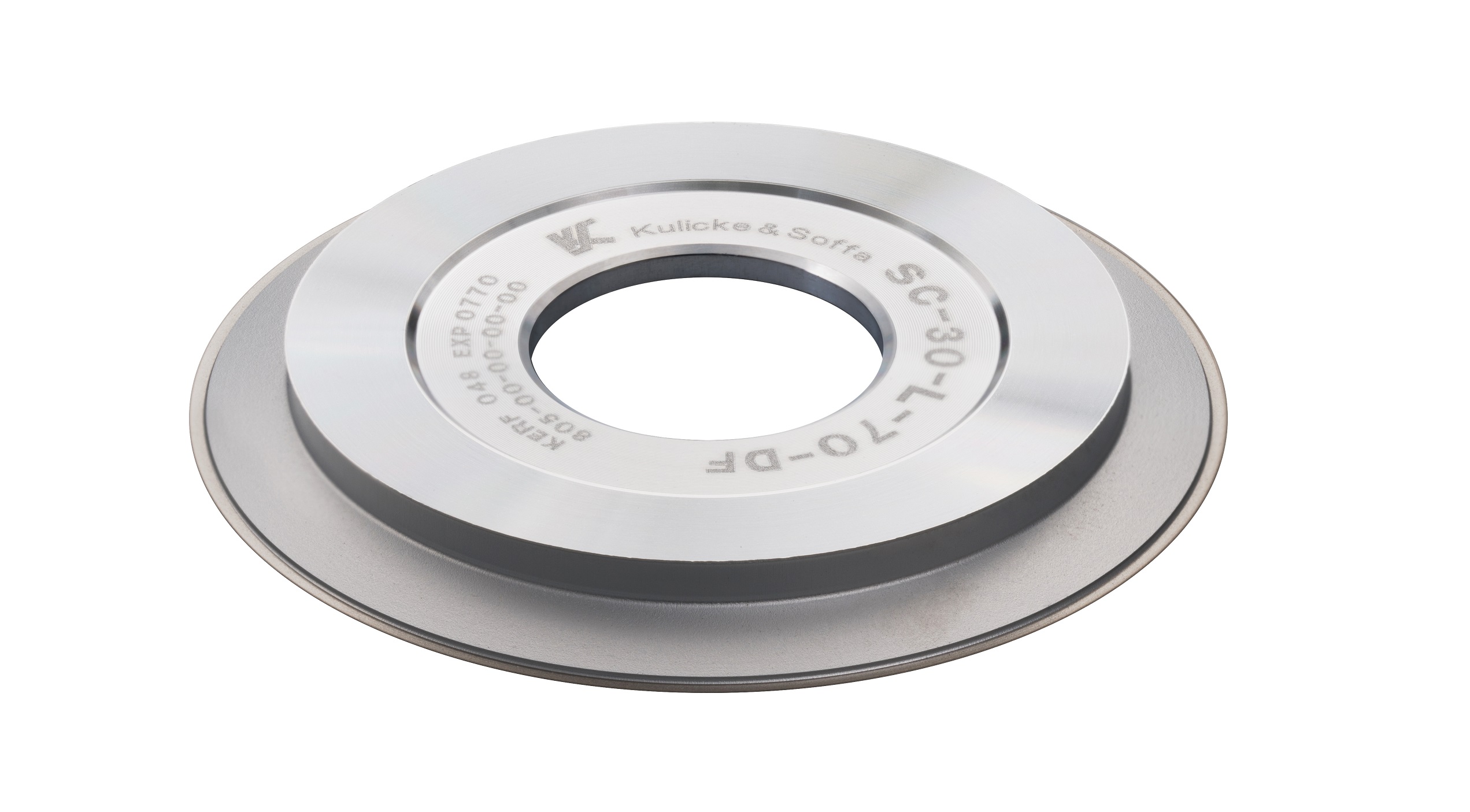
HCL Hub Blades
The new K&S HCL (High Competitive Line) Hub Blades series offers superior quality and valuable features that make it a highly competitive alternative to silicon wafer dicing – particularly for discrete, logic IC & LCD drivers.
These new silicon dicing blades provide competitive pricing, standardization and consistency.
- Offering the finest aluminum edge
- Grooved surface to improve cut debris removal
- Consistent exposure due to smooth aluminum edge finishing
They deliver quality, precision and COO improvement as a result of the following new features:
- New aluminum hub provides improved production throughput and extended blade life.
- In addition, it supports thinner blades and kerf for narrow saw street silicon wafer dicing.
- Enhanced in-house blade dressing that improves diamond exposure and controls blade eccentricity.
- HCL Hub Blades cut and wear very consistently and demonstrate improved vibrational control.
- More consistent top side chipping performance.
- Shiny hub provides enhanced visual control.
Application Examples for HCL Hub Blades
K&S HCL Hub Blades are appropriate for a wide range of applications. The most common applications include the following:
- Logic IC (silicon wafer dicing): 200 – 500um thick wafer dicing
- Discrete (silicon wafer dicing): 150 – 400um thick wafer dicing
- FlipChip (Fanout, CoWos, WLP): 500 – 800um thick wafer dicing (single cut after laser grooving)
- LED Package Singulation: Ceramic 100 – 800um EMC (epoxy molding compound)
- DFN, BGA Package Singulation: 0.5 to 1.5mm substrate thickness
Contact Cheryl Martin at (267) 999-1266 to learn more today!